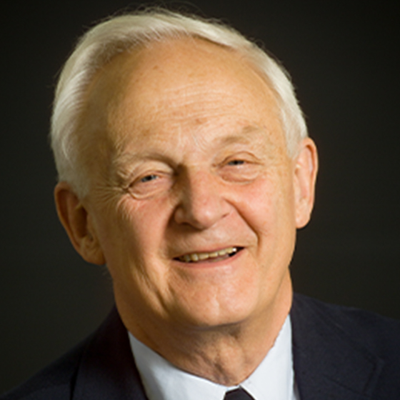
John Silcox
Biography
Silcox joined the Cornell faculty in 1961 and has twice served as director of the School of Applied and Engineering Physics, and as director of the Materials Science Center. He spent sabbatical leaves as a Guggenheim fellow in France and England in 1967–68, at Bell Laboratories in 1974–75, and at Arizona State University in the spring term of 1983. He is a fellow of the American Physical Society and a member and past president of the Electron Microscopy Society of America, from whom he received the 1996 Distinguished Scientist Award in physical sciences. For 1978 through 1982 he served on the Solid State Sciences Committee of the National Academy of Sciences/National Research Council. In 1988 he was named the David E. Burr Professor of Engineering. Silcox has been a member and chair of the Materials Research Advisory Committee for the National Science Foundation, and also served on advisory committee to the Arizona State University (high resolution). He is chair of the Steering Committee for the Electron Microscopy Center at Argonne National Laboratory. In 1998 he was appointed as the Vice Provost for Research for the Physical Sciences and Engineering.
The driving theme of our program is the exploitation of atomic size electron beam coupled with electron spectroscopy to determine electronic-structural features on an atomic scale. Typical questions addressed in the recent past include the growth of thin-film structures, bonding at interfaces in metals and meta/ceramic hetero-interfaces and the strain and atomic distributions in quantum wells and wires. Quantum dots are coming under study at present. This provides atomic precision maps of the electron scattering in the sample (typically given by the atomic structure). Electrons elastically scattered to large angles locate the electron probe precisely on the sample and the energy loss electrons give the electronic structural features. The problem areas that can be tackled with this approach impacts a wide range of solid state and materials physics problems (see publication list below. Critical to understanding the observations is accurate simulation of the propagation of the electron beam through the thin-film sample is critical to accurate interpretation of the observations and there is an ongoing effort in collaboration with Dr. Earl J. Kirkland at improving the understanding of electron scattering. Data is acquired digitally and is therefore directly available for quantitative analysis.
With this approach it has proven possible to separate amorphous sp2 bonded carbon from diamond, silicon carbide from silicon oxide and silicon, all with a 5 Å spatial resolution. This was important in understanding the growth processes. Strains have been measured around quantum wires embedded in GaAs. It proved possible to measure the lattice parameters on about a 20 Å area to +/- 0.005 Å level. This proved valuable in establishing that observed shifts in the photoluminescence were due to strain rather than quantum confinement. Finally, electron energy loss spectra in 3d transition metal systems reflect local changes in the unoccupied d-density-of-states. These in turn can be shown to reflect changes in the bonding at the boundaries and thus, eventually, to give quantitative estimates of increases in the heat of formation at the boundaries. Finally, these estimates are used to provide an electronic structure contribution to the grain boundary energy for use in criteria that determine the transition from inter to trans granular failure. Copper/magnesium oxide interfaces have been studied and GaN/AlGaN interfaces are currently under study. New insights into silicate glass/ metal interfaces have been obtained and extensive studies of radiation damage in silicate glasses reveal the precipitation of tiny metallic spheres that alter the optical properties.
A new electron scattering instrument based on aberration correctors for electron lenses is under design and construction which is expected to achieve 1 Å probe size and 0.3 eV energy resolution is under design and construction. It is expected to arrive at Cornell c. 2003-2004.
Research Interests
- Glass based interfaces (National Science Foundation –MRSEC) - Other participant; Z.Yu, graduate research assistant.
- Semiconductor Interfaces (Office of Naval Research) - Other participants: K.A.Mhkoyan, graduate research assistant
- Development of a 1 Å electron scattering probe (National Science Foundation)
Selected Publications
- Muller, D. A., Y. Tzou, R. Raj, and J. Silcox. 1993. Mapping sp2 and sp3 states of carbon at a subnanometer spatial resolution. Nature 366:725–27.
- Muller, D. A., S. Subramanian, P. E. Batson, S. L. Sass, and J. Silcox. 1995. Near atomic scale studies of electronic structure at grain boundaries in Ni3Al. Physical Review Letters 75(26):4744–47.
- Golden, J. H., F. J. DiSalvo, J. M. J. Frechet, J. Silcox, M. Thomas, and J. Elman. 1996. Subnanometer diameter wires isolated in a polymer matrix by fast polymerization. Science 273:782–84.
- D.A. Muller, D.A. Shashkov, R.Benedek, L.H.Yang, D.N.Seidman and J.Silcox, “Chemistry and Bonding at {222}MgO/Cu Heterophase Interfaces”, Phys. Rev. Letts., 80: 4741-4744 (1998).
- M.J. Plisch, J.L. Chang, J. Silcox, R.A. Buhrman, , “Atomic-scale characterization of a Co/AlOx/Co magnetic tunnel junction by scanning transmission electron microscopy” Appl. Phys. Lett., 79, 391–393
- Ozatay, Ozhan, Praveen G. Gowtham, K. W. Tan, J. C. Read, K. A. Mkhoyan, M. G. Thomas, Gregory David Fuchs, Patrick M. Braganca, Eric M. Ryan, K. V. Thadani, John Silcox, Daniel C. Ralph, Robert Buhrman. 2008. "Sidewall Oxide Effects on Spin-Torque and Magnetic-Field-Induced Reversal Characteristics of Thin-Film Nanomagnets." Nature Materials 7 (7): 567-573.

